Saturday, 15 August 2015

BLINKING LED AND GETTING STARTED PROBLEM IN AREDUINO


This was my first Arduino program. The simplest: Blinking LED!

Yes it might sound very easy for a person whose done a couple of experiments. But for an absolute beginner, I faced these few problems.

1) The driver was not finding COM5/COM6 PORT.
2) When I was done with the first problem, a new problem came out. COM 6 is already in use.

How to solve it. 
1) Search for VCP drivers.
2) Download the compatible driver according to your OS.
http://www.ftdichip.com/Drivers/VCP.htm

3) Then watch this video

https://www.youtube.com/watch?v=Ozrxs7rIeRM

FOR BLINKING LED

/*
  Blink
  Turns on an LED on for one second, then off for one second, repeatedly.

  Most Arduinos have an on-board LED you can control. On the Uno and
  Leonardo, it is attached to digital pin 13. If you're unsure what
  pin the on-board LED is connected to on your Arduino model, check
  the documentation at http://arduino.cc

  This example code is in the public domain.

  modified 8 May 2014
  by Scott Fitzgerald
 */


// the setup function runs once when you press reset or power the board
void setup() {
  // initialize digital pin 13 as an output.
  pinMode(13, OUTPUT);
}

// the loop function runs over and over again forever
void loop() {
  digitalWrite(13, HIGH);   // turn the LED on (HIGH is the voltage level)
  delay(1000);              // wait for a second
  digitalWrite(13, LOW);    // turn the LED off by making the voltage LOW
  delay(1000);              // wait for a second
}

Friday, 14 August 2015

Keypad Interface with 8051

Matrix Keypad

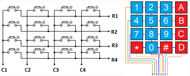
Matrix Keypads are commonly used in calculators, telephones etc where a number of input switches are required. We know that matrix keypad is made by arranging push button switches in row and columns. In the straight forward way to connect a 4×4 keypad (16 switches) to a microcontroller we need 16 inputs pins. But by connecting switches in the following way we can read the status of each switch using 8 pins of the microcontroller.
4x4-Matrix-Keypad
4×4-Matrix-Keypad
The status of each keys can be determined by a process called Scanning. For the sake of explanation lets assume that all the column pins (Col1 – Col4) are connected to the inputs pins and all the row pins are connected to the output pins of the microcontroller. In the normal case all the column pins are pulled up (HIGH state) by internal or external pull up resistors. Now we can read the status of each switch through scanning.
  1. A logic LOW is given to Row1 and others (Row2 – Row-4) HIGH
  2. Now each Column is scanned. If any switch belongs to 1st row is pressed corresponding column will pulled down (logic LOW) and we can detect the pressed key.
  3. This process is repeated for all rows.


Keypad Interface Code:   
#include<reg51.h>


sbit rs = P3^5;
sbit e = P3^6;

void delay(unsigned int x)
{
while(x--);
}

void cmd(unsigned char c)
{
P3 = c;
rs = 0;
rw = 0;
e = 1; 
delay(50);
e = 0;
}

void dat(unsigned char b)
{
P3 = b;
rs = 1;
rw = 0;
e = 1; 
delay(50);
e = 0;
}


void lcd()
{
cmd(0x38);
delay(300);
cmd(0x80);
delay(300);
cmd(0x0E);
delay(300);
cmd(0x01);
delay(300);
}

void main()
{
int a,b,c;
lcd();
while(1)
{
P1 = 0x0F;
while(P1 == 0x0F);
a = P1;
P1 = 0xF0;
b = P1;
while(P1!=0xF0);
c = a+b;
if(c==0xE7)
{
dat('7')
delay(60000);
cmd(0x01);
}  
else if(c==0xEB)
{
dat('8')
delay(60000);
cmd(0x01);
}
else if(c==0xED)
{
dat('9');
delay(60000);
cmd(0x01);
}
else if(c==0xEE)
{
dat('/');
delay(60000);
cmd(0x01);
}
else if(c==0xD7)
{
dat('4');
delay(60000);
cmd(0x01);
}
else if(c==0xDB)
{
dat('5');
delay(60000);
cmd(0x01);
}
else if(c==0xDD)
{
dat('6');
delay(60000);
cmd(0x01);
}
else if(c==0xDE)
{
dat('*');
delay(60000);
cmd(0x01);
}
else if(c==0xB7)
{
dat('1');
delay(60000);
cmd(0x01);
}
else if(c==0xBB)
{
dat('2');
delay(60000);
cmd(0x01);
}
else if(c==0xBD)
{
dat('3');
 
delay(60000);
cmd(0x01);
}
else if(c==0xBE)
{
 
dat('-');
delay(60000);
cmd(0x01);
}
else if(c==0x77)
{
 
dat('C');

delay(60000);
cmd(0x01);
}
else if(c==0x7b)
{
 
dat('0');

delay(60000);
cmd(0x01);
}
else if(c==0x7D)
{
dat('=');

delay(60000);
cmd(0x01);
}
else
{
dat('+');
delay(60000);
cmd(0x01);
}
}
 }


Interfacing keypad with 8051 microcontroller (AT89S52)

4x4 matrix keypad


The same code simulated in Proteus looks like this: 


SEVEN SEGMENT DISPLAY (SSD) INTERFACE ON 8051


SEVEN SEGMENT DISPLAY (SSD)

It is an output device and this is how it looks like so don't get confused when you face it as you're about to get familiar with it in the most basic way. Don't worry, I will explain the output pins soon enough.

Seven Segment Display (SSD)

As you can see, it's called Seven Segment Display because it has actually got Seven Segments (that's too obvious I guess). These seven segments can be used to display different shapes but it is designed such that it's meaningful to display only numbers on it. And this is how they will actually look like


SSD Output (Numbers)

You can think of the segments as individual LEDs which can be turned ON/OFF. There you are, I just told you the working secret behind it. So when it comes down to LEDs, you already know that it looks like this

LED Symbol

And I hope you also know that it will glow ONLY when current flows from ANODEtowards CATHODE. Before moving forward, you can read my article about LEDs and interfacing them to 8051 if you want to know more about them. However, let's stay focused on SSD here. SSDs are also composed of individual LEDs and work on the very same principle. So basically they come in two forms

  1. Common Anode
  2. Common Cathode
Common Cathode

Common Anode


Pin Description of SSD

FOR COMMON CATHODE
  • Connect INPUT VOLTAGE to A
  • Connect GROUND to COMMON (either upper or lower as both are shorted) 

FOR COMMON ANODE
  • Connect INPUT VOLTAGE to COMMON
  • Connect GROUND to A


8051 SSD INTERFACE

Till now, you might have noticed that displaying something on the SSD is all about giving it the right type of sequence. The SSD itself is just a combination of LEDs. It's your job to know what you're doing. For instance, you have to turn ON segment 'b' and 'c' for displaying '1' (verify from above diagram). You require seven control lines to completely utilize an SSD for display i-e a, b, c, d, e, f, and g (dot is optional). As for the common pin, connect it to

  • GROUND for Common Cathode
  • 3-5V for Common Anode

For interfacing it with 8051,you can use 74LS47 IC. It is basically BCD to 7-segment Decoder/Driver which is specially designed for driving an SSD. It's function is such that it gives out the corresponding sequence for SSD when the microcontrollers sends a number 0-9. You can find more details about the IC in it's Datasheet Here is the truth table for common cathode configuration

BCD to 7-SEGMENT Decoder Truth Table 

As you can see, providing the number (0-9) as INPUT will produce the correspondingSEQUENCE at its output which is used to display that number on the SSD. However, I'm not going to use this IC for interfacing. Why complicate things by introducing some extra hardware when you can manage it through software? I am going to present an interfacing scheme for SSD which doesn't include any other component. I won't keep you waiting, here it is

8051 SSD Interface

And trust me when I say it, it's as simple as it looks. Nothing more, nothing less. I have directly connected the SSD to 8051 because the MCU don't have the 'guts' to damage it and the program code can take care of the sequences which is even more simpler! You can have a look by yourself

SSD Interface C language Code

Also have a look at the Proteus Simulation diagram.The input at PORT1 shows 00000101 (binary) which is and thus the output at SSD is also 5

Proteus Simulation Diagram

LCD INTERFACE ON 8051


LCD

Stands for Liquid Crystal Display and is definitely an output device. It comes in many popular shapes and sizes but here is the one that you will most probably face at the beginner's level.

COMMON LCD
COMMON LCD
Let's focus on this one. It is basically called 16x2 LCD because it has sixteen columns and two rows thus it can display thirty-two (32) characters at a time (sixteen characters in each row). There are sixteen hardware pins as shown.

LCD HARDWARE PINS
LCD HARDWARE PINS


Number
Pin
Function


1
GND
Ground
2
Vcc
Power Source (+5V)
3
Vee
Contrast Control
4
RS
Register Select
0=Command Register
1=Data Register
5
R/W
Read/Write
0=Write
1=Read
6
E
Enable
7-14
D0 – D7
8-bit data pins
15
BL+
Backlight Control
16
BL-
Ground


PINS

The RS  (Register Select) control pin is used to select either command or data register as described in the pin configuration table. Once selected, all data sent on the 8-bit data lines will be latched to that register.

The R/W (Read/Write) control pin is used to determine the flow of data. You have to select

  • Write Mode when you're sending something to the LCD (data or command)
  • Read Mode when you're reading from the LCD

The E (Enable) control pin acts as a guard to allow exchange of data. This pin is very important in this whole process and must be handled precisely. The following animation explains its function


SENDING DATA TO LCD

 Commands:


LCD INTERFACE CODE:

Naming each pin using #define
Naming each pin using #define
  •  I created two separate functions. As you can see, the only difference is that of using RS pin according to requirement.

LCD Command Function
LCD Data Function
LCD Data Function

  • The delay function is a general one and you can use it safely at this stage but remember that it's not accurate. 
Delay Function
Delay Function

  • Here is my main function

LCD Main Function
LCD Main Function


Here is the Proteus Simulation Diagram for LCD interface.:
Proteus Simulation
Proteus Simulation


Thursday, 13 August 2015

SWITCH INTERFACE ON 8051


SWITCHES

Switches come in many different shapes and sizes. The main idea or function is to either enable or disable something by simply turning it on/off. Thus it acts as an input device that users can use to control certain parts of the system. Below are the most common switches that you will come across

Push Button

ON-OFF Switch


In circuit diagrams, a switch is generally represented by 

Switch Symbol

After examining the Switch Symbol, I think it is quite clear how a switch actually works. It closes (connects) or opens (disconnects) a circuit. The Push Button behaves in the same fashion as it closes the circuit as long as you keep holding it in pressed state.  


SWITCH INTERFACE CODE

Here is the C language code for the Switch Interface with the 8051 microcontroller-

SWITCH Interface C Language Code
Let me explain the code in a step wise fashion

  • PIN1.0 is renamed as sw using  (for convenience)
  • Similarly PIN1.1 is renamed as led (LED is connected to this pin)
  • sw is declared as input pin (for reading switch status)
  • led is declared as output (for driving LED on/off)
  • if ( !sw ) statement is true only if switch is ON (sw = 0 and !sw = 1) and thus led will glow
  • Otherwise led will stay OFF

The same code simulated in Proteus looks like this -

Proteus Simulation
This concludes the topic for today. I hope that after reading this post, you have at least some basic idea of using a switch with the 8051 microcontroller. 


LED TOGGLE PROGRAM CODE ON 8051


LED TOGGLE

LED (Light Emitting Diodes) are simple lights that you can turn ON/OFF. They glow when they are ON and they don't when they are not. They look somewhat familiar to the picture below

Standard RED LEDs

Program Code:
C LANGUAGE CODE


The delay function used in this code is also a general one and it roughly provides the required delay in milliseconds as defined by the input parameter. So we are talking of one second when we say delay(1000). You can use this function for now but don't ever use it when timing is crucial and you need more accuracy. 

Here is the simulation design for PROTEUS that I used. As I said, I wouldn't care much about the resistor. Neither in the simulation nor in practical scenario.

PROTEUS SIMULATION DESIGN

I have also included the design file in the download package. I hope that this post has given you an idea of how things are done in real. It gets easier with practise. Any suggestion/feedback is highly appreciated as I might have missed something. Remember that there is always an easier way around in programming so I encourage you to learn, understand and then venture on your own adventure. Goodluck for the implementation. 


HOW TO USE KEIL

HOW TO USE KEIL

Finally you have decided to write your own code for the 8051 microcontroller. It doesn't matter whether you have chosen Assembly or C Language for yourself but what matters now is that you need an environment specially designed for 8051. Basically you are looking out for IDE (Integrated Development Environment) that will help you build and compile programs. While there are many options out there, I prefer KEIL uVision in this regard.


KEIL IDE is basically an assembler and a compiler or whatever you name it. You can write either an Assembly or C language code and KEIL will take care of the rest for you. Furthermore, it supports many of the 8051 variants that you will face. You can download KEIL from their official website using the link below.


After successful download and install, you may have problem getting familiar with it if you're using it for the very first time but don't worry because I am here to give you a graphical tutorial on how to use it for writing your program, compiling it, and finally generating the HEX file.

Here we go


PROJECT > NEW uVISION PROJECT

Give some name and click SAVE

when prompted, select proper device that you're using ( i-e ATMEL > AT89C51 )

When prompted, select YES

Click NEW button and write your code (Assembly or C language)

SAVE the file with proper extension as above


Right click SOURCE GROUP 1 as shown


Go to options for the project

Enable HEX file generation

Build the project

Use this HEX file to program your IC

These are the simple steps for a successful compilation and generation of HEX file. Now I hope you have created your first HEX file and ready to program it to the 8051. And you know how to do that, right? If your answer is no then please check this out.

UPDATE:

If you have trouble understanding the pictures then here is a video of the same process that I made. Hope you get a better view this time